








For over six decades, the modern digital economy has been built on a single, extraordinarily abundant element: silicon. From the guidance computers of the Apollo missions to the hyperscale server farms training trillion-parameter artificial intelligence models today, silicon-based microchips have driven the most rapid expansion of technological capability in human history. By etching billions of microscopic transistors onto wafer-thin slices of refined silicon, semiconductor engineers faithfully delivered on Moore’s Law—doubling computing density every two years while slashing costs.
That golden era of silicon-driven exponential growth has collided with the unyielding laws of physics and thermodynamics. As transistor dimensions shrink to atomic scales, silicon is reaching its structural limits. Below two nanometers, physical phenomena such as quantum tunneling cause electrical current to leak uncontrollably across transistor gates, turning idle processing cores into heat generators. At the same time, the global explosion of AI workloads, cloud computing, and autonomous systems has turned microchips into one of the world’s most power-hungry industrial outputs. Global data centers now consume massive amounts of electricity annually, with a significant fraction of that energy dissipated purely as waste heat.
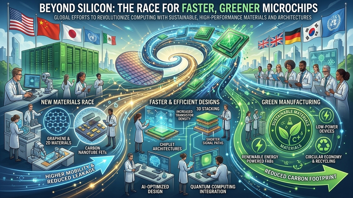
The semiconductor industry faces a historic dual mandate: computing must become dramatically faster to handle high-dimensional algorithms, but it must simultaneously become vastly greener to prevent the digital revolution from overwhelming global energy grids. The race is on to discover, scale, and commercialize alternative materials and architectures capable of superseding silicon. From single-atom-thick two-dimensional crystals to optical computing and carbon nanotube arrays, a multi-front revolution is underway to build the microchip of tomorrow.
The Cracks in the Silicon Foundation
To understand why the semiconductor industry is searching for alternatives, one must look at what happens inside a silicon transistor at the atomic level. A transistor acts as an ultra-fast electronic switch. Applying a voltage to the gate electrode creates an electric field that draws charge carriers—electrons or positive “holes”—through a underlying channel, turning the switch “on.” Removing the voltage stops the flow, turning it “off.”
For decades, engineers shrunk these components by simply reducing the channel length and thinning the gate oxides. However, when the silicon channel becomes only a few atoms thick, the material loses its ability to control electron flow. Electrons begin to jump across the barrier even when the switch is nominally turned off, a phenomenon known as gate leakage.
This leakage creates two severe operational barriers:
- The Power Wall: Energy is continuously wasted as heat even when the microchip is performing no active computation, forcing processors to throttle their operating speeds to prevent physical destruction.
- Mobility Degradation: At extreme sub-nanometer dimensions, the speed at which electrons travel through silicon—known as carrier mobility—drops drastically due to atomic-level scattering against channel boundaries.
Compounding this physics crisis is an environmental one. The energy footprint of modern computing has reached an unsustainable trajectory. Training a single frontier AI model consumes gigawatt-hours of electricity, while the manufacturing of advanced silicon wafers requires millions of gallons of ultra-pure water, hazardous chemical solvents, and high-temperature furnaces operating continuously at over 1,000 degrees Celsius.
The industry can no longer rely on brute-force miniaturization of silicon. Continuing the march toward faster, energy-efficient computing requires fundamental innovations in material science.
The Contenders: 2D Materials and Atomic Engineering
Among the most promising candidates to replace silicon in digital logic chips are two-dimensional (2D) materials—crystalline structures consisting of a single layer of atoms. Unlike bulk silicon, which suffers from severe electrostatic degradation at atomic thicknesses, 2D materials retain exceptional electrical, optical, and mechanical properties even when trimmed down to sub-nanometer profiles.
The two primary classes of 2D materials leading the post-silicon race are Transition Metal Dichalcogenides (TMDs) and graphene derivatives.
Transition Metal Dichalcogenides (TMDs)
While graphene famously demonstrated astronomical electron mobility, its lack of a natural bandgap—the energy barrier required to cleanly turn an electronic switch on and off—makes it unsuitable for traditional digital logic. TMDs, such as Molybdenum Disulfide (MoS₂) and Tungsten Diselenide (WSe₂), overcome this hurdle.
TMDs possess a natural, well-defined bandgap alongside an ultra-thin body thickness of less than one nanometer. This atomic thinness provides superior electrostatic control, effectively suppressing short-channel effects and eliminating gate leakage even at gate lengths below two nanometers. Leading research consortia and major foundries have demonstrated functional MoS₂ field-effect transistors that achieve carrier mobilities far exceeding equivalent silicon architectures, paving the way for logic gates that operate at higher switching speeds while drawing a fraction of the power.
Carbon Nanotube Field-Effect Transistors (CNFETs)
Another frontrunner in atomic engineering is the carbon nanotube—rolled-up sheets of single-layer graphene that form microscopic, hollow cylinders. Carbon nanotubes conduct electricity with near-zero electrical resistance, allowing electrons to zip through the channel ballistically without generating friction-induced heat.
Transistors built from aligned arrays of carbon nanotubes promise up to a ten-fold improvement in energy efficiency and a three-fold increase in processing speed compared to advanced silicon nodes. Commercial foundries are working to translate CNFET technology from laboratory prototypes to industrial fabrication lines, integrating carbon nanotube logic directly on top of standard silicon wafers to create high-density 3D hybrid chips.
Sub-2nm Scaling Challenge (Silicon)
        ↓
Quantum Tunneling & Severe Gate Leakage
        ↓
Alternative Channel Solutions
   ├── 2D TMD Materials (MoS₂ / WSe₂) → Atomic-layer electrostatic control
   └── Carbon Nanotubes (CNFETs) → Ballistic electron transport with minimal heat
Wide-Bandgap Power Electronics: GaN and SiC
While 2D materials target the ultra-dense, low-voltage logic processing found in CPUs and GPUs, a parallel material revolution is transforming power management, electric vehicles, and industrial energy systems. Here, the goal is not to pack billions of transistors onto a thumbnail-sized die, but to handle extreme voltages, high temperatures, and high electric currents with near-zero energy loss.
Silicon is notoriously inefficient at high voltages, breaking down thermally and electrically under heavy load. Enter wide-bandgap (WBG) compound semiconductors, chief among them Gallium Nitride (GaN) and Silicon Carbide (SiC).
- Gallium Nitride (GaN): GaN features an electronic bandgap nearly three times wider than that of silicon, allowing it to withstand much higher electric fields before breaking down. GaN transistors switch tens of times faster than silicon counterparts with dramatically lower internal resistance. In practical terms, this enables power converters that are smaller, lighter, and run much cooler. GaN is already replacing bulky silicon power bricks with ultra-compact consumer chargers, while rapidly expanding into 5G radio-frequency power amplifiers and data center power distribution units.
- Silicon Carbide (SiC): Capable of operating at temperatures exceeding 500 degrees Celsius and managing voltages in the thousands, SiC has become the preferred material for high-power industrial applications. In electric vehicles (EVs), replacing silicon inverters with SiC power modules increases driving range by 5 to 10 percent while cutting charging times significantly. Furthermore, SiC inverters reduce energy conversion losses in utility-scale solar farms and wind turbine grids, directly accelerating the global transition toward renewable energy.
By minimizing resistive heat loss across power distribution systems, wide-bandgap semiconductors offer one of the most immediate avenues for reducing global electricity consumption.
Photonic Computing: Replacing Electrons with Light
One of the fundamental inefficiencies of modern microchips is that data transfer relies on moving physical electrons through copper wires and silicon traces. As clock speeds increase, resistance in these metallic interconnects generates substantial heat and introduces latency bottlenecks—a dilemma known as the RC (resistance-capacitance) delay.
Photonic computing solves this problem by replacing electrons with photons. By guiding pulses of light through microscopic waveguides etched into the chip surface, data can be transmitted at the speed of light with virtually no heat generation or electromagnetic interference.
Traditional Electronic Interconnects
Attacker → Moving Electrons Through Copper → High Resistance → Heat & Thermal Throttling

Integrated Photonic Architecture
Attacker → Guiding Photons Through Waveguides → Zero Resistance → Near-Instant, Cool Data Transfer
The initial deployment of this technology centers on Silicon Photonics and Co-Packaged Optics (CPO). Rather than replacing electronic logic entirely, optical interconnects replace the power-hungry electrical pathways that link memory chips, processor cores, and server racks together.
In hyperscale data centers, co-packaged optics allow GPUs and specialized AI accelerators to share data across optical fibers instantaneously, reducing interconnect energy consumption by up to 70 percent. Looking further ahead, full optical neural networks—where mathematical matrix multiplications are calculated directly using the interference patterns of light beams—promise to run complex artificial intelligence algorithms thousands of times faster than electronic digital processors while consuming a fraction of the watt.
Beyond von Neumann: In-Memory, Neuromorphic, and 3D Integration
Material innovation alone is insufficient if computing platforms remain trapped in legacy architectural designs. For seventy years, computer design has been dominated by the von Neumann architecture, which physically separates the central processing unit (CPU) from memory storage (RAM).
In modern data-intensive workloads, moving data back and forth across the narrow bus between memory and processor consumes up to 80 percent of a microchip’s total energy budget—a structural bottleneck known as the “memory wall.”
To create genuinely greener microchips, the industry is combining alternative materials with non-von Neumann architectures:
In-Memory and Memristive Computing
Rather than continually shuttling data to the processor, in-memory computing executes mathematical operations directly within the memory array itself. Using novel materials such as transition metal oxides and phase-change compounds, engineers build memristors—resistors with memory that alter their electrical resistance based on applied voltage history. Memristive arrays perform analog computations, such as weighting parameters in an artificial neural network, directly at the location of data storage, eliminating data transfer energy entirely.
Neuromorphic Chips
Inspired by the biological human brain, which processes complex sensory tasks using less power than a standard household lightbulb, neuromorphic architectures discard traditional clock cycles. Instead, they rely on event-driven, spiking neural networks. Neuromorphic microchips utilize 2D materials and specialized memristive switches that remain completely silent when idle, firing electrical spikes only when new input data arrives, drastically reducing standby power draw.
Monolithic 3D Integration
Because physical limits prevent chips from growing horizontally, manufacturers are stacking logic, memory, and sensor layers vertically in a single, monolithic 3D structure. By utilizing cold-temperature deposition of 2D materials and carbon nanotubes, engineers can build layers of logic directly on top of memory banks without melting the delicate wiring below. This vertical integration shortens data interconnect distances from millimeters to nanometers, accelerating throughput while reducing power dissipation.
The Manufacturing Hurdle: From Lab to Fab
While the theoretical advantages of post-silicon materials are unquestioned, translating breakthroughs from university cleanrooms into commercial fabrication facilities presents a monumental engineering challenge. The modern semiconductor manufacturing ecosystem represents the most refined industrial pipeline on Earth, representing trillions of dollars in specialized infrastructure optimized exclusively for silicon.
Introducing new materials into existing silicon foundries creates significant hurdles:
- Material Purity and Wafer Uniformity: Growing a single-atom-thick monolayer of MoS₂ or aligning billions of carbon nanotubes perfectly across a 300-millimeter industrial silicon wafer requires extreme chemical precision. Microscopic defects, grain boundaries, or atomic voids can render an entire batch of microchips useless.
- Thermal Budgets and Contamination: Many emerging materials require synthesis temperatures exceeding 800 degrees Celsius, which can melt underlying copper wiring on pre-processed wafers. Furthermore, foundries are intensely cautious about introducing new chemical elements that could contaminate multi-billion-dollar ultra-clean fabrication tools.
- Process Design Kit (PDK) Development: Chip designers rely on complex software simulation models to layout integrated circuits. Transitioning to 2D materials or photonic logic requires building entirely new electronic design automation (EDA) frameworks and physics models from scratch.
To bridge this “lab-to-fab” gap, major semiconductor foundries, equipment suppliers, and international research institutes like imec are establishing dedicated pilot lines for 2D materials and advanced packaging. Between 2025 and 2030, advanced node roadmaps from leading foundries increasingly feature hybrid architectures—embedding 2D material channels, wide-bandgap power modules, and optical interconnects directly onto back-end-of-line (BEOL) silicon processes.
A Heterogeneous Future
The race for faster, greener microchips will not yield a single winner that completely eradicates silicon overnight. Silicon’s low cost, structural abundance, and decades of manufacturing optimization guarantee it will remain a workhorse for standard, low-cost computing applications for years to come.
Instead, the future of microelectronics is inherently heterogeneous. Tomorrow’s computing platforms will be modular, composite systems—a specialized ecosystem where different materials perform the specific tasks to which they are naturally suited.
A single advanced processor will feature a silicon base substrate, 2D material channels for sub-nanometer logic scaling, embedded carbon nanotube arrays for ultra-fast cache memory, co-packaged optical interconnects for cool data transmission, and Gallium Nitride power modules managing energy delivery with near-zero loss.
The transition beyond silicon marks a historic turning point in human technological development. By moving past the physical boundaries of bulk silicon to embrace atomic-layer physics, optical communication, and brain-inspired architectures, the semiconductor industry is breaking free from the constraints of the power wall. The race for post-silicon microchips will not only expand the limits of computational performance, but will ensure that the digital foundation of human progress remains sustainable, efficient, and green for generations to come.